


Not Just Relocation, but Reshaping: Why 2026 is the Critical Turning Point for the PCB Supply Chain

AI-generated - A PCB connected to an AI server.
Key Takeaways
- 2026 marks the shift from factory relocation to yield-driven competition in PCB manufacturing
- High-layer AI boards are pushing copper plating chemistry to its operational limits
- Southeast Asian expansion introduces new risks in chemical consistency and process control
- Material purity is becoming a qualification factor for global electronics customers
If 2024 and 2025 represented the migration period for global PCB manufacturing, 2026 marks the moment when relocation turns into operational reality. New factories will no longer be judged by construction speed, but by yield stability, chemical control, and the ability to support advanced copper plating processes required by AI-driven electronics.
Relocating equipment is straightforward compared to stabilizing electroplating chemistry. High-layer-count boards, deep vias, and ultra-fine circuitry place unusual stress on plating baths. Under these conditions, raw material quality is no longer a purchasing decision alone. The purity and dissolution behavior of Copper Oxide directly influence plating uniformity, bath lifetime, and defect rates.
The 2026 supply chain realignment is far more than a geographic shift; it is a fundamental chemical and technical transition. This pivotal moment determines whether new production bases can master the material precision needed to meet the rigorous reliability standards of next-generation electronics.
The New Southeast Asian Powerhouses: From Construction to High-Yield Production
The rapid expansion of PCB facilities in Thailand, Malaysia, and Vietnam has created impressive capacity on paper. However, by 2026, the critical question will shift from sheer volume to process maturity. In this evolving landscape, Pan-Continental Chemical offers a diverse and resilient supply chain with strategic production bases in Taiwan, China, and Vietnam. With a combined capacity exceeding 2,000 tons per month, we provide not just scale, but the technical stability and reliability standards essential for next-generation electronics.
Thailand: Scaling Continuous Copper Plating
Thailand’s projected rise to the world’s fifth-largest PCB hub by 2026 reflects a qualitative pivot in the global supply chain. No longer confined to the automotive sector, Thai manufacturing is aggressively moving up the value chain into high-end domains such as AI infrastructure and LEO satellites. By 2026, the narrative shifts from 'Thai-made capacity' to 'Thai-made reliability' for next-generation electronics.
Malaysia and Vietnam: Precision Manufacturing Pressure
Malaysia’s semiconductor ecosystem is attracting substrate and high-end HDI manufacturers. These processes operate at micron-scale tolerances where plating chemistry stability is critical. Copper oxide must dissolve predictably to maintain a stable ion balance, especially during long production runs.
Vietnam’s concentration in HDI and flexible circuits brings another challenge: microvia reliability. Fine-feature plating is highly sensitive to particulate contamination. Inconsistent oxide sources increase the probability of nodules, uneven grain structure, and micro-cracks that only appear during thermal cycling tests.
As these regions mature, the limiting factor is no longer machinery. It is chemical consistency across batches and across suppliers.
The Geopolitical Entry Ticket
For cloud infrastructure providers and advanced electronics brands, regional diversification is now a baseline requirement. Qualification audits increasingly examine upstream chemical supply reliability. A factory without stable access to high-purity plating materials is seen as a production risk regardless of equipment investment.
Chemical supply chains are becoming part of geopolitical eligibility. This shift elevates material producers into a strategic role within the PCB ecosystem.
The Technology Triad: AI, ASIC, and LEO Demand Material Purity
The next wave of electronics is defined by performance density. AI servers, custom ASIC platforms, and low Earth orbit satellite systems all push PCB fabrication beyond historical norms.
Industry Pressure Summary
|
Industry Driver |
Manufacturing Pressure |
Chemical Requirement |
|
AI and ASIC platforms |
Extreme aspect ratio vias |
High-purity copper oxide for stable copper ion balance |
|
LEO satellites |
Thermal cycling reliability |
Consistent purity to prevent structural micro-defects |
|
800G and 1.6T telecom |
Signal integrity sensitivity |
Smooth and uniform copper deposition |

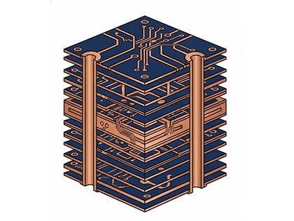
AI-generated - Schematic diagram of a high layer count PCB.
1. AI and ASIC: Extreme Layer Counts and Deep Via Challenges
Prototype AI accelerator boards already approach layer counts that strain conventional plating chemistry. As aspect ratios increase, copper must deposit uniformly across deep vias without trapping voids or creating uneven wall thickness.
High-purity copper oxide dissolves cleanly and maintains a stable copper ion supply. Inferior material introduces particulates that alter current flow and produce irregular grain growth. The result is reduced via reliability under thermal and electrical stress.
For expensive AI infrastructure, a single plating defect can invalidate an entire board. Yield protection begins at the chemical level.
The expansion of custom ASIC platforms further intensifies these requirements. HDI and substrate-like products demand tighter grain control and smoother copper profiles to preserve signal integrity at high frequencies.
2. LEO Satellites: Reliability Under Thermal Extremes
Satellite electronics must endure rapid temperature cycling and intense radiation. In such harsh environments, PCB reliability depends on more than just metallization quality—it requires a flawless bond between the copper and the substrate.
The integrity of these connections is highly sensitive to the purity of the plating bath. Any undissolved residues or metallic impurities from low-grade copper oxide can create structural weaknesses that lead to delamination or cracking during extreme thermal expansion and contraction.
3. Telecom Infrastructure and Signal Integrity
The leap toward 800G and 1.6T network systems places extraordinary demands on signal integrity. As we move into these ultra-high frequencies, the "skin effect" becomes dominant, meaning signals travel primarily along the surface of the copper.
- Controlled Roughness: Ultra-low-loss substrates require copper surfaces with precisely controlled roughness to minimize signal attenuation.
- Surface Morphology: Plating uniformity begins with stable bath chemistry. Copper oxide that dissolves unevenly creates fluctuations in deposition behavior, leading to microscopic surface irregularities.
- Electrical Design Integration: At high frequencies, these microscopic flaws translate into measurable signal loss. Material consistency, therefore, has become a core component of electrical design, moving beyond simple chemical management.
Conclusion: The Blurring Boundaries
As chiplet architectures expand and substrate-like PCB technologies spread into edge computing, the historical boundary between substrates and HDI boards continues to fade. Manufacturing environments must handle complexity once reserved for semiconductor packaging.
The winners of 2026 will not simply be factories that relocated successfully. They will be organizations that understand the link between chemical inputs and system-level reliability. High-end electronics manufacturing is moving toward a model where supply chain control and materials science operate as a single discipline.
Pan-Continental Chemical supports this transition by focusing on copper oxide engineered for advanced electroplating environments used in modern PCB copper plating applications. In an era defined by density, speed, and thermal stress, chemical precision is no longer optional. It is the foundation of manufacturable innovation.